Engineered to mitigate electrostatic hazards and shield sensitive semiconductor components globally.
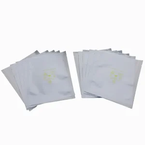
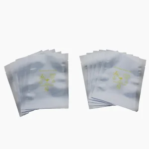
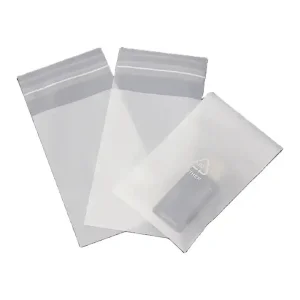
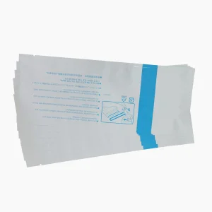
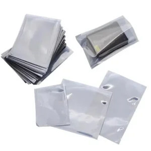
In the modern microelectronics, semiconductor, and aerospace manufacturing sectors, electrostatic discharge (ESD) represents one of the most persistent, financially destructive, and chemically complex failure modes. An ESD event as low as 100 volts—far below the threshold of human perception—can instantly rupture silicon substrates, melt gate oxide layers, and induce latent defects in integrated circuits (ICs) that compromise performance post-delivery. As global supply chains shift toward high-yield, zero-defect quality programs, the strategic procurement of ESD-safe packaging solutions has migrated from a secondary procurement process to a fundamental engineering requirement.
A common misconception in commercial electronic procurement is conflating "anti-static" properties with "static shielding" properties. Fully understanding the physical differences between these classifications is vital for protecting high-value logic devices during cross-border transit:
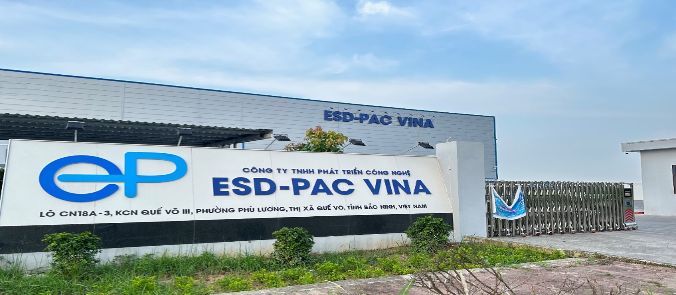
Founded in March 2018, ESD-PAC VINA has rapidly emerged as an international leader in the engineering, design, and high-volume manufacture of technical foil structures, anti-static films, aluminum laminate pouches, and vacuum bags. Headquartered in the bustling industrial ecosystem of Quy Vu Industrial Park, Bac Ninh Province, Vietnam, we maintain a state-of-the-art 12,000 square meter factory designed to meet the rigorous cleanliness and environmental control standards required by the tech manufacturing industry.
By blending state-of-the-art co-extrusion technology with integrated research, development, manufacturing, and direct global sales channels, we control every critical phase of the packaging development cycle. This vertical integration allows us to serve as a reliable, transparent partner for OEMs and EMS providers globally, providing them with materials engineered to protect high-cost electronic assets.
To deliver reliable protection against triboelectric charge, physical abrasion, and atmospheric moisture, ESD-PAC VINA designs and manufactures high-performance ESD bags utilizing a sophisticated multi-layer laminate construction. Each layer plays a distinct structural role:
| Layer Component | Material Formulation | Primary Function & Electrostatic Characteristic |
|---|---|---|
| Outer Layer | Dissipative Polyester (PET) | Resists triboelectric charging; controls exterior dissipation paths ($10^6$ to $10^{10} \ \Omega/\text{sq}$). |
| Shielding Layer | Vapor-Deposited Aluminum (or Foil) | Creates the Faraday Cage effect; blocks external electrostatic fields and discharges. |
| Reinforcement Layer | Biaxially Oriented Nylon (ONy) | Improves puncture resistance, tear strength, and mechanical toughness during shipping. |
| Inner Layer | Dissipative Polyethylene (PE) | Facilitates airtight heat sealing; prevents static generation when products slide within. |
Our manufacturing technology utilizes high-accuracy co-lamination to prevent layer delamination under conditions of high humidity, thermal fluctuations, or long-term vacuum sealing. Our bags maintain surface resistivity levels of $10^6$ to $10^{11} \ \Omega/\text{sq}$ across temperature variations, ensuring compliance with global electronics shipment standards.

Our operational philosophy is built on two core principles: precision engineering and environmental stewardship. A packaging failure during shipping can lead to damaged electronic components, resulting in costly scrap, warranty claims, and significant ecological waste. At ESD-PAC VINA, we view high-performance packaging as an essential element of modern corporate sustainability.
To reduce our carbon footprint, our Quy Vu Industrial Park operations utilize energy-efficient machinery, run solvent recovery systems, and recycle processing scrap wherever possible. We are dedicated to delivering packaging solutions that help global brands protect their valuable electronic equipment while minimizing environmental impact.
As microelectronics shrink, they become increasingly sensitive to static discharges. The demand for customized ESD and moisture barrier packaging solutions spans multiple global high-tech industries:
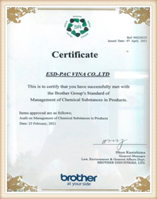
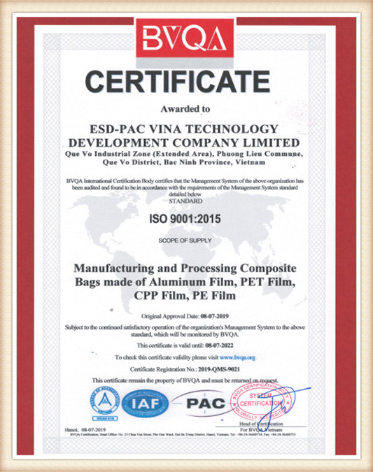
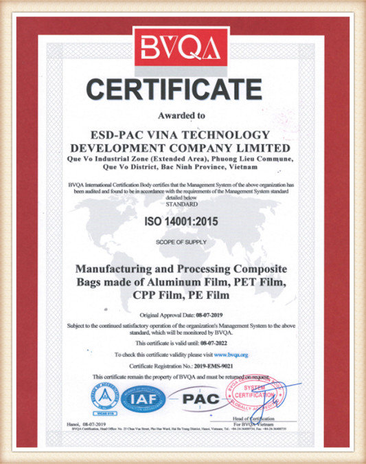
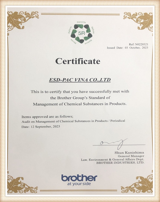
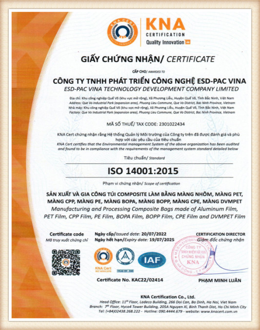
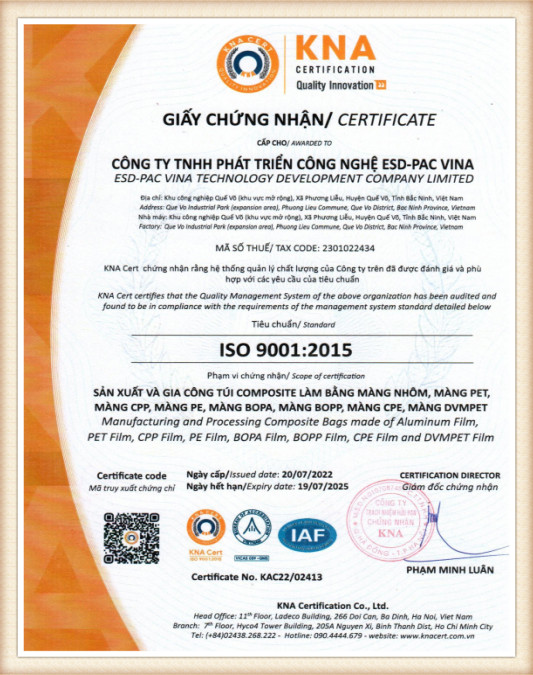
Our state-of-the-art facilities and material formulations undergo regular, independent validation to meet international quality, environmental safety, and performance standards.
As semiconductor packaging advances toward sub-2nm nodes, wafer-level chip scale packaging (WLCSP) and 3D stacking require increasingly sensitive ESD controls. Traditional ESD packaging contains topical antistatic coatings that can transfer trace chemical contaminants (such as outgassed amines, silicones, and heavy metal ions) to delicate electronic components. Our research and development efforts are focused on three main pillars:
Technical insights and purchasing guidance regarding ESD and static shielding applications.
Explore our standard and custom ESD packaging options. Contact our engineering team for custom sizing, printing, and thickness specifications.
 ESD-PAC VINA